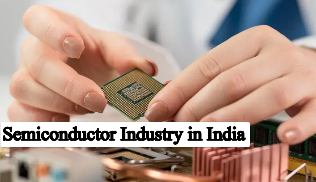
India’s semiconductor sector will reach a critical point in 2025. The ecosystem is finally beginning to produce tangible results after years of announcements and policy formulation. India Semiconductor Mission, allied incentive programs and state-level policy are combining with global supply chain changes and domestic demand in order to reshape India’s semiconductor landscape.
Key Drivers
1. Strong domestic demand & market growth
The Indian semiconductor market will be worth around US$ 55-55 billion by 2025. Forecasts predict that it will more than double to US$ 110-110 billion by 2030.
Sectors like consumer electronics, automotive electronic, IoT, and telecom (5G/6G) are driving growth. The industry is aware of the impact that supply chain disruptions in the past (e.g. During COVID-19, India’s vulnerability was exposed due to its dependence on imported critical chip and materials components.
2. Government Policy & Incentive
India Semiconductor Mission plays a central role. It offers grants linked to performance, capital subsidies and state facilitation in the form of land, power, and water.
PLI schemes (Production Linked Incentive Schemes) complement ISM, by encouraging investments in fabs and design, as well as testing, packaging, and testing.
To attract investment, several states have implemented policies on semiconductors or electronics manufacturing. Andhra Pradesh is a prominent example. Gujarat, Punjab and Tamil Nadu are also important.
3. New manufacturing capacity & First homegrown chips
The government has approved multiple semiconductor manufacturing projects (fabrication, ATMP and OSAT), some of which are already in construction.
The first Indian semiconductor chip will be available by 2025. It will be manufactured by Tata Electronics and PSMC in partnership with the Dholera fab, Gujarat, under the Semicon India program.
4. Roadmap to Advanced Nodes
India has outlined a 5-7-year roadmap for achieving production at 7 nanometer (nm). Partnerships like IBM and IMEC are being considered for advanced R&D as well as technology transfer and capability building.
Initial fabs will produce at nodes that are coarser (e.g. 28 nm is still relevant in many applications, such as automotive, display driver chips and so on.
5. Focus on Ecosystem – Design, Packaging and Materials, Human Capital
There is increasing attention to the upstream and downstream value chains, including: design/IP; advanced packaging & tests; compound semiconductors (e.g. SiC), materials, chemicals, equipment, gases.
In order to support this, government and industry organisations are developing programmes for skilling and education. A push is being made to include MSMEs, startups, and academia in the design, prototyping, and R&D.
Key Challenges
Despite the positive momentum, there are still many challenges to overcome.
1. Node Complexity & Technology
Capital-intensive and technically complex, moving to advanced nodes (such as 7 nm or 5 nm) requires clean-rooms and lithography tools. It also requires highly-skilled manpower. India is only just starting to develop this capability.
2. Supply Chain Dependence
Imports include materials, precursor chemicals and specialty gases as well as high-precision machinery. It will take some time to build local/regional supply chains and requires coordinated investment.
3. Financing & Capital Intensity
The initial investment required for semiconductor fabs, especially those at the leading edge, is huge (land, infrastructure and machines). The return on investment is slow, but incentives can help. Investors require clarity, regulatory stability and risk mitigation. Geopolitical risk is a major concern for investors.
4. R&D & Skilled Workforce
A shortage of qualified talent exists in the fields of semiconductor physics and engineering, materials science and lithography. To scale up this talent, we need training institutions, R&D laboratories, and collaborations.
5. Time Lag & Execution Risks
Many projects have been announced, and some are in construction. But, it will take years to turn these announcements into actual functioning fabs or production volumes, yields of quality, etc. It will take many years. There is a possibility of delays, cost overruns, or issues with technology transfer.
6. Global Competition and Geopolitical pressure
China, Taiwan, South Korea, USA and other EU countries are also heavily investing. India should find its niche, rather than trying to do everything all at once (could involve mid-to mature nodes or specialty semiconductors or packaging/testing).
What To Watch In 2025 & The Near Term (Next 2 Years)
- If the “first Made in India Chip” (28 to 90 nm) is delivered as promised before 2025. This will serve as a test of India’s planning and execution, as well as its quality, yields, etc.
- How many fabs / ATMP / OSAT facilities become operational (not just under approval/construction).
- India’s progress on the 7-nm roadmap will depend on whether it is able to secure the necessary partners, IP/licensing and equipment, as well as whether the domestic production of supporting material ramps up.
- More startups and academic institutions are doing tape-outs, more IP is being produced in the country and better access to design tools.
- Workforce Development Initiatives: Licensing, certification and degrees related to the semiconductor process. Collaborations with universities.
- Execution at the state level: States such as Gujarat and Odisha will compete with each other to attract fabs. State policies in relation to water, land and regulatory clearances, power, will be important.
- Global supply chain alignment – whether India can connect to supply chains of US, Taiwan, EU, etc., particularly for packaging, testing, and materials.
Strategic Implications & Business Analysts’ Take
- For investors There are significant opportunities in midstream (packaging testing and design) where India is more able to scale quickly. The leading-edge fabs, however, will be more risky but could also have high rewards. Diversification among nodes, regions, and applications will reduce risk.
- For Domestic Industry & Startups : This may be the best opportunity yet to build domestic IP, get access to incentives and leverage government support. But execution discipline will be crucial (quality, yield and timelines).
- For Policymakers: It is important to have stable policies, consistent incentives, and streamlined clearances. This will help avoid delays with inter-state infrastructures (power, roads, water). It is also important to promote the localization of skills and materials.
- For global firms India offers demand, improved infrastructure, incentives, as well as a skilled workforce at a lower cost. India is a good partner for semiconductors (for R&D, packaging/testing, fabrication or R&D).
Outlook
By the end of 2025 India will likely have achieved several milestones that are symbolic and fundamental: first in-house chip production, multiple fabs/OSAT/ATMP under production or close to it, increased design activity, improved incentive, better infrastructure readiness at state level. The journey to become a global powerhouse in semiconductors (especially for cutting-edge nodes) is going to take a sustained effort over the next 5 years or more.
India can carve out niches in many areas (e.g. SiC, power semi-conductors, packaging/testing/IP/design are all viable niches for India to carve out. If the country can manage to align policy, investment and human capital with global demand as well as supply chain and supply chain, it will become a trusted player in global semiconductor value-chains (not only a consumer market).